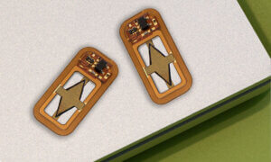
Researchers at Stanford University and MIT found a way to reduce the bottleneck created by moving data from one chip to another. Their new system is a 3D chip design developed with carbon nanotubes and RRAM #hardwaremagic
As more data is released in the wild, the need to store it and process it correctly and fast increases. Unfortunately, the current system that takes care of those two tasks implies moving data back and forth, from the storage chip to the computing one. When the connection falters or goes slower, it inevitably creates a bottleneck. So, MIT researchers thought of a way to go around this problem.
The team used carbon nanotubes and resistive random-access memory to create a nanoelectronic chip design with 3D architecture. The choice of materials was closely related to the temperatures they support – below 200 degrees Celsius. Normally, to manufacture 2D transistors you need at least 1,000 degree temperatures. But at 200 degrees though, you can juxtapose an extra layer on top.
This was critical because it gives the chip the power to combine logic AND memory components. Plus, the materials used are more energy-efficient that standard ones. Not to mention, the top layer has the capability of acting like a sensor, feeding data to the layers below.
This new design paves the way for advanced data processing locally, so where the sensors are placed.
Follow TechTheLead on Google News to get the news first.


